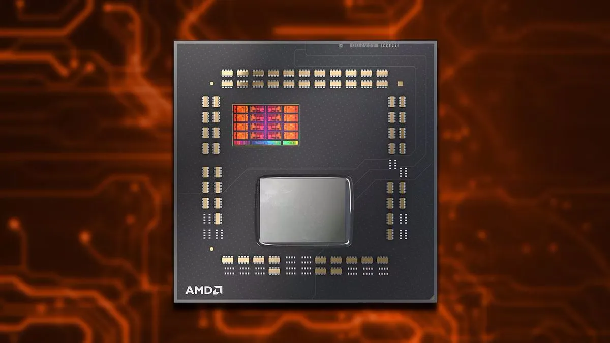
So that’s where the higher clock speeds and better thermals stem from.
You must log in or register to comment.
Would make a lot of sense to me.
- L3 would connect on one side to the cores, but on the other to the memory controllers. In this configuration the memory connection won’t need to go back to the CCX die only to get routed directly to the IO die.
- With the CCX die on top, it should make getting the heat out of it a lot easier. It’s no longer got the L3 die sitting on it like a blanket.
The drawback is that there’s probably more logic on the L3 die to be able to deal with all signals passing from the CCX to other chiplets.


