
Hey everyone!
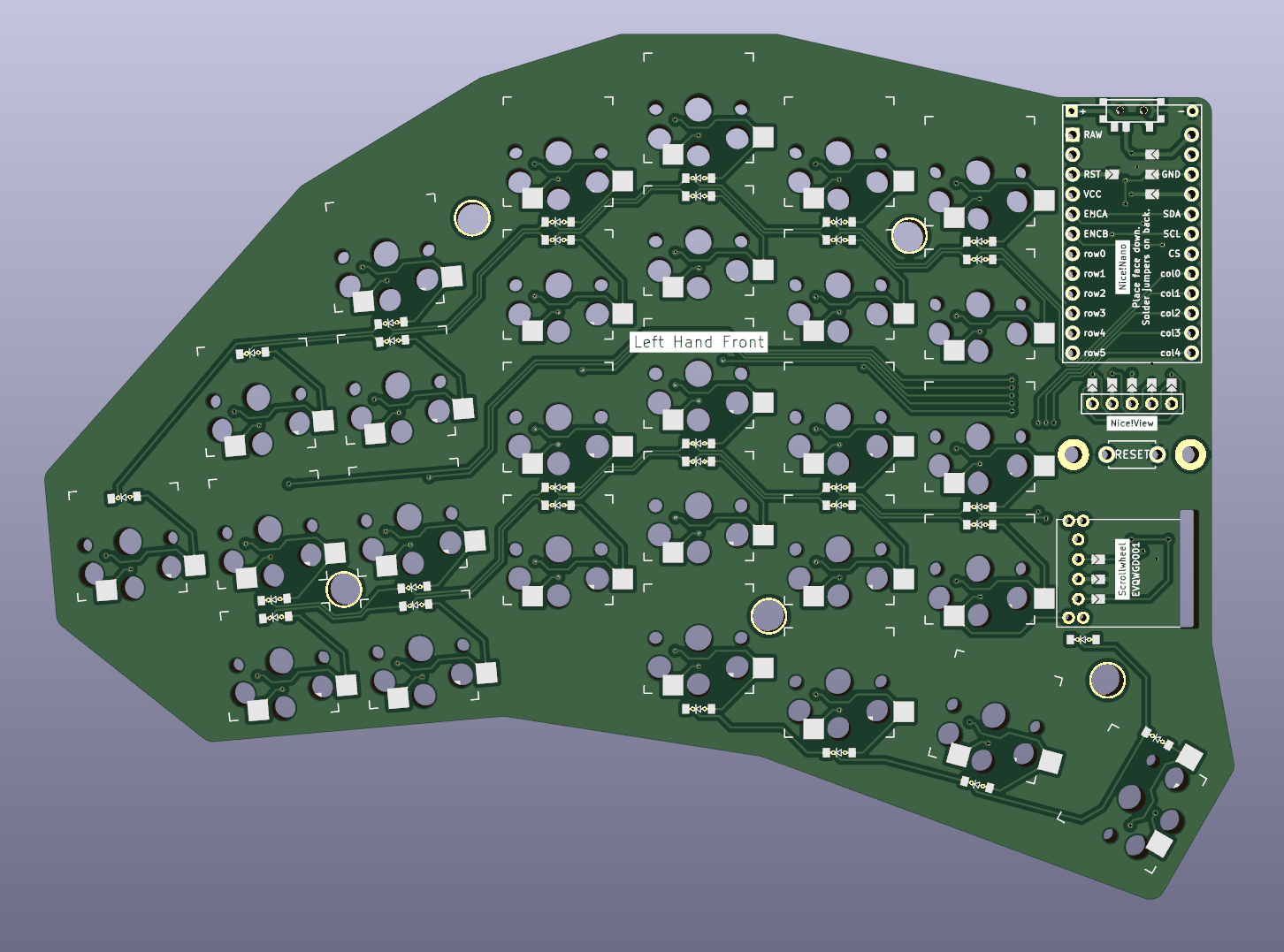
I jumped into the ergomech rabbit hole sometime last year and after using a sofle as my daily driver since then, I now decided it’s time to build my own “thing”. After going through endless revisions to figure out what I actually want, and trying to learn how to trace PCBs, this is what I have come up with: A choc-spaced 56 keys wireless build with a scrollwheel and some staggering.
It’s a reversible PCB. To make this work with single pin hole for both sides, I used jumpers for pins that can not be set in software (VCC, GND, RST). For rows/columns, I plan to do a different mapping in software to not have a jumper for every single pin.
All files including the kicad_pcb and ergogen config are available and open source at github: https://github.com/dnlbauer/splitkeyboard .
However, this is the first thing I ever designed. Therefore, I was hoping if you guys could have a look at the PCB before I get it etched and point out if there are any obvious errors?
Of course, I am also happy about any feedback in general. :)
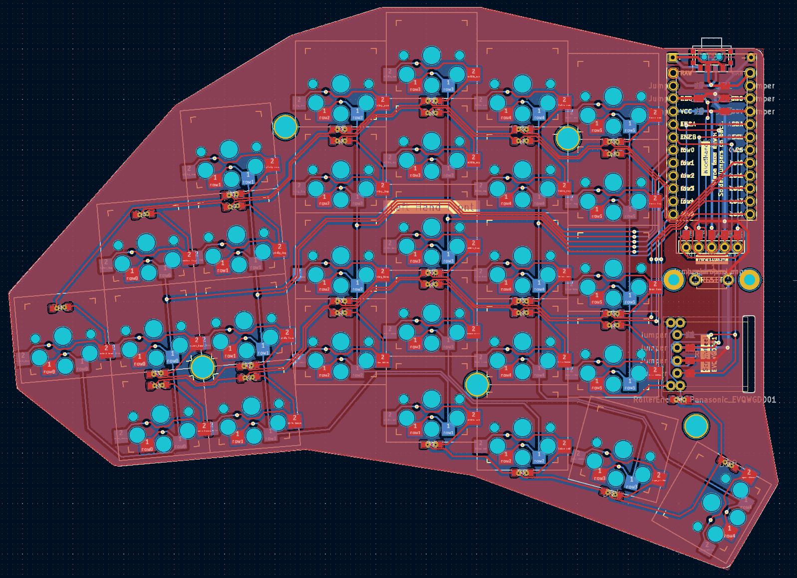
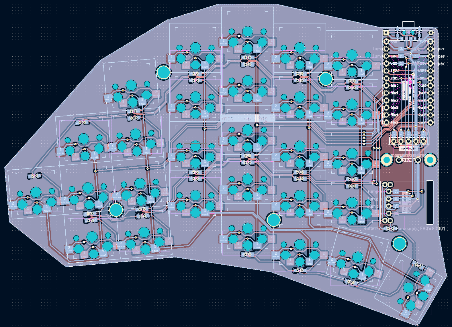
I’ll give things a look over. First thought, you ground poured, but didn’t link any of it together with vias. That would be helpful in ensuring good ground return paths.
Yeah just some vias for return to ground; everything looks reasonably fine from a quick overview. You have space, and cross talk really isn’t a concern, but more padding between signal traces could be helpful in some of the closer areas. Though all of that is minimal in concern.
I just kept the default value (I think its 0.2mm) between traces. I could probably double it at some points where multiple traces are bundled though. Thanks for the hint!
thanks for the imput. Do you mean I should just place some random vias to connect both sides of the ground plane? To be honest, I dont understand exactly what this ground plane is used for since none of the traces actually connect to it. Is it merely for shielding against signal noise?
I’m no electrical engineer. But I was informed that having the return to ground close to all data connections is a good thing from a EMI and signaling perspective. I often put ground vias near all my rows and column pads.
Are you in the Absolem Discord? They can probably help you confirm everything looking right.
good idea!
Interesting design. Wish I could produce something that works for me.
I’m not a designer or engineer.
Only error I noticed is the “.” at the end of your url
https://github.com/dnlbauer/splitkeyboard.<- leads to 404.
fixed the domain. thanks for pointing that out!
If you are interested in the design process, I can highly recommend the tutorial series by FlatFootFox here. It was a great resource for me to get started. https://flatfootfox.com/ergogen-introduction/
Hi, this looks interesting to me. I will happily take a look at this for you. Do you have the KiCad schematic file as well (with file extension “.kicad_sch”)?
Hey, unfortunately erdogen, which I used to generate the starting point for the pcb does not generate a schematic file. It only generates the PCB and ratsnest for the footprints. So I dont have one. I think I could create one though. Mind telling me what this is used for and why one should have one?
It’s mostly useful for reference. If I open up both the PCB file and the schematic file, clicking on one element of the PCB will highlight the same item in the schematic, so I can double-check connections.

![[PCB Review Request] A choc-spaced 56 key wireless build](https://lemmy.world/pictrs/image/da52a9d0-adef-4700-98df-0d3bda9f5735.jpeg)